VSCP register addressing
 VSCP uses registers to read and write information to and from a node. This article describes the way the addressing of these registers works in VSCP. It describes the mapping of registers in the MDF to the node’s application space and the way the application in turn stores these registers.
Overview
Addressing of registers in VSCP is defined in two locations; the Module Description File and the vscp_node_defines.h files in the firmware.
The Module Description File describes the functionality of a node, the registers that are used to access this functionality and the events that a node generates and responds to. The file is in XML format. The intended use is for application software to be able to get information about a node and its functionality in an automated way. In this article I’ll explain how to build a custom MDF for the Mespelare VSCP node.
The MDF’s format is XML, so it is easy to read by humans as well as machines. I recommend using Notepad++ to edit the MDF. In this article we’ll be using different MDF files from the internet as the basis to build our own node’s MDF. The VSCP specification has some good information and examples about the MDF.
Application vs. VSCP reserved registers
The VSCP standard makes a distinction between application registers and VSCP reserved registers. Application registers are specific to the application running in the node, and are entirely defined by the node’s manufacturer. Such registers include application configuration registers, status registers, result value registers etc.
VSCP reserved registers are fixed registers which are defined by the standard and cannot be changed by the manufacturer. These registers are used for the configuration of the protocol. Such registers include the location where the MDF is stored (its URL), user ID values, manufacturer ID’s, the node’s GUID etc.
Register addressing
Under the <registers> tag, all application registers used by the node are described. The VSCP reserved registers are not described, but are implied by the VSCP standard and the software that uses it (e.g. VSCPworks).
Each register has two properties that address the register, the page and the offset. The page describes on which register page the register is placed. Each page can hold 256 registers (0 - 254 decimal). The first 128 registers on each page, 0 - 127 decimal, are used for application registers. The next 128 registers, 128 - 254 decimal, hold the VSCP reserved registers. So every page holds 128 application and 128 reserved registers. One specific quirk of the addressing scheme which is worth mentioning, is that there are only 128 reserved registers and that they are simply duplicated on each page. So for example reading page 6 registers 127 to 254 will yield the same results as reading page 0 registers 127 to 254.
The MDF described the registers in decimal format.
The Decision Matrix is stored in application register space and must be defined in this space by the MDF, as we’ll see later on.
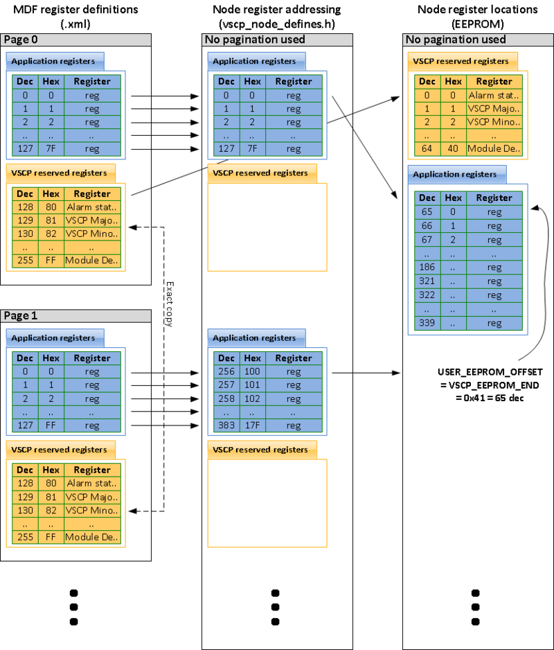
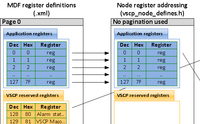
In the above register model the left side shows the registers as described in the MDF. Clearly shown is the pagination of the registers into two pages, page 0 and page 1. In the MDF this will be described as:
<!-- DM Row 1 -->
	<reg page="0" offset="0">
Where page=”0” is the page number, and offset=”0” is the first register on this page. The last application register that can be described on a given page will be offset=”127”.
The middle of the register model shows how these registers are mapped onto the register space in the application (i.e. how the firmware running on the node sees and stores them). Here the mapping for the Hasselt (and Mespelare) nodes are shown as an example. Different applications/nodes may/will make this mapping in different ways.
As you can see the application doesn’t see nor store the VSCP reserved registers. And it doesn’t use pagination, it simply puts the registers from all pages in consecutive order. For simplicity it does leave a gap where the VSCP reserved registers would be. These registers are stored to and read from EEPROM memory within the PIC microcontroller.
To map the registers to locations, the application uses labels defined in vscp_node_defines.h.
#define REG_DESCISION_MATRIX		0	// Start of matrix, 256 = page 1:0
#define DESCISION_MATRIX_ELEMENTS	10  // # of DM registers = # elements * 8

#define EEPROM_ZONE					80  //Zone node belongs to
#define EEPROM_SUBZONE				81  //Subzone node belongs to

#define REG_STATUS_OUT1				82  //Output status register 1
#define REG_STATUS_OUT2				83  //Output status register 2

...

//The following registers are on page 1
#define REG_PTIME_OUT1				256 // RW Output protection timer
#define REG_PTIME_OUT2				257 // RW Output protection timer
Registers on page 1 would be defined in the MDF as
<!-- Output protection time register (#define REG_PTIME_OUTx) -->
<reg page="1" offset="0" >
	<name lang="en">Relay protection time register for relay 1 (REG_PTIME_OUT)</name>
Effectively one can convert from MDF register to the register address used by the application using the formula
application register addressing = MDF page * 256 + MDF offset
One needs to describe each application register in the MDF with the correct page and offset, and this needs to correspond with the registers defined in the vscp_node_defines.h file of the firmware. The register descriptions are terminated by a </registers> tag.
The Decision Matrix
The DM is a special case of application registers. It is described outside of the <registers> tags, but rather inside <dmatrix> tags. The DM registers are addressed in the same way as the application registers, this means that for addressing purposes they can be considered as part of the application registers.
<!-- Decision matrix -->
<dmatrix>
	<level>1</level>
	<start page="0" offset="0"/> <!-- REG_DESCION_MATRIX -->
	<rowcnt>10</rowcnt> <!-- DESCION_MATRIX_ELEMENTS -->
Here the first DM register is described as page 0, offset 0, which maps to application register 0. So in the vscp_node_defines.h file of the firmware we would find:
#define REG_DESCISION_MATRIX	   0	// Start of matrix, here page 0 offset 0
#define DESCISION_MATRIX_ELEMENTS  10   // # of DM registers = # elements * 8
The DM registers are not described individually in the firmware. Instead only the first register location is described, and how many DM rows are available. Since each DM row has 8 registers, the last DM register in this case would be located at location 79 (10 * 8 - 1). Thus the next available location for the following register is 80.
Other application addressing concerns
vscp_node_defines.h defines a few labels that relate to register addressing:
#define USER_EEPROM_OFFSET VSCP_EEPROM_END
VSCP_EEPROM_END in turn is defined as:
#define VSCP_EEPROM_END   0x41	// marks end of VSCP EEPROM usage
					            // = next free position (so last used register + 1)
This label defines the location of the next free position after the last VSCP reserved register in application space (EEPROM), and is used to offset the application registers after the VSCP reserved registers.
This effect can be seen on the right-hand side of the register model. In EEPROM first the VSCP reserved registers are stored, followed by the application registers.
#define USER_EEPROM_LAST_POS 121
This label defines the position used by the last application register. It is used to test if a register read request should be handled by the vscp_readAppReg() function or the vscp_readRegister() function. I believe the current implementation of the vscp_readAppReg() in the Hasselt firmware doesn’t handle paginated application registers.